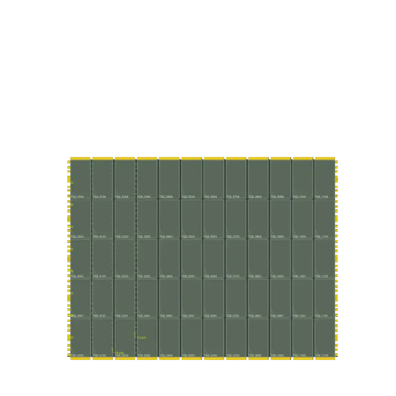
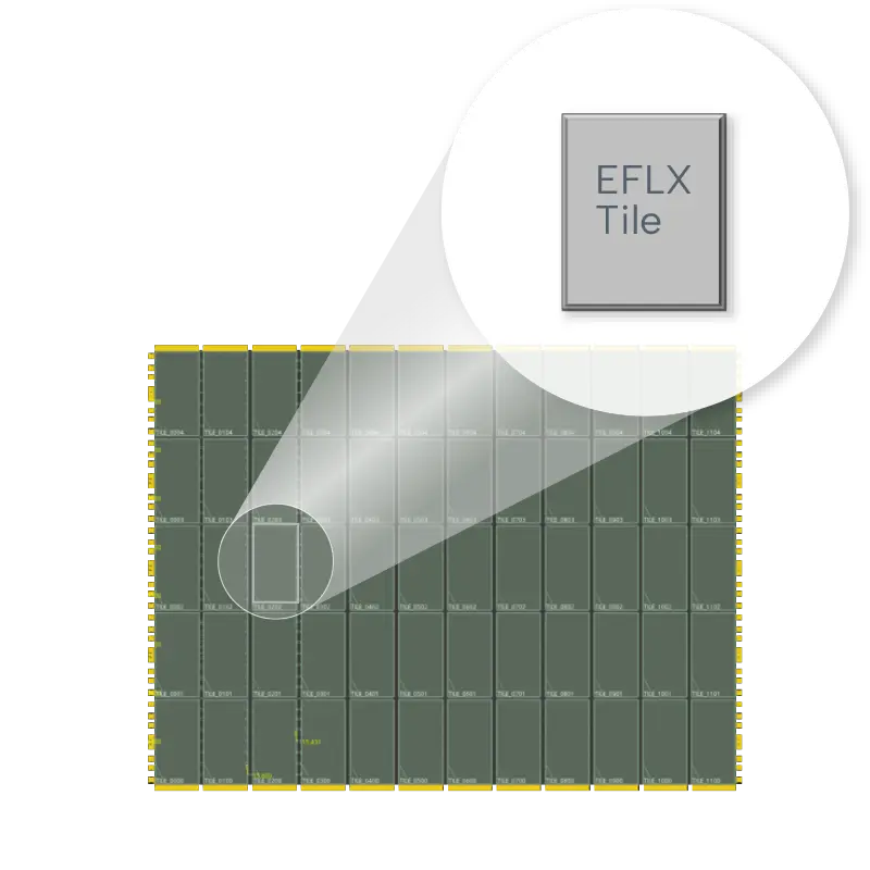
Modular Architecture
Get the exact eFPGA you want
- Get the size, features and process node you want.
- EFLX® tiles come in 3 types: all-logic, 1/4 DSP MAC and 3/4 logic, and extra IO.
- EFLX tiles automatically connect when tiles abut due to our top-level mesh. We mix tiles of different types to give you exactly what your application needs. 240K LUTs (see right) is the largest array so far. >1M LUTs coming in 2023.
Process Nodes
Get the process node and metal stack you want
eFPGA is silicon proven today in TSMC 40nm, 28nm, 16nm, 12nm and available on 7/6nm. 5nm and 3nm are in development.
eFPGA is also silicon proven today on GlobalFoundries 12nm and available now on 22FDX.
Intel 18A development is scheduled to start in Q2 2024.
Because of our proprietary interconnect we use only a few metal layers more than the standard cell library of the foundry so we support most metal stacks.
Contact us for specifications such as silicon area, metal stacks, leakage power, etc.
If you need a node not currently available, we can develop EFLX eFPGA on any node in ~6 months from contract and resource availability.
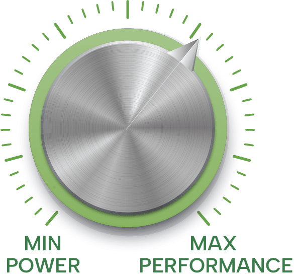
Power vs Performance
We can optimize for what matters most
Our advanced process nodes are optimized for maximum performance because customers designing on those nodes care about speed the most. In N7 for example we run 500MHz+ over SS to FF and -40C to +125C Tj.
Larger geometry nodes are typically used for more power sensitive applications.
Renesas’ ForgeFPGAs on 40nm burn just milliwatts. We can do high-VT design, power gating, state retention and other power management features for minimum energy consumption.
Or we can implement for a balance between power and performance. You decide.
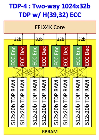
Reconfigurable Block RAM
Reconfigurable Block RAM
Most customer EFLX eFPGA arrays include Block RAM.
But customers have a wide range of features they want that they either had to implement themselves in Verily (complexity and LUTs) OR we implemented in a custom way costing time and $.
Now we have a Reconfigurable Block RAM.
Choose between true dual port, two port or single port access (True Dual Port is shown to the right).
- Tradeoff memory depth and width as desired
- Add automatic parity or error detection/correction
- Implement write enables on a partial word basis if needed
Competitive Advantage
EFLX eFPGA Competitive Advantage
We deliver the widest range of sizes, features and nodes at the best power/performance/area compared to our competitors.
This is because of patented interconnects: XFLX™ uses half the transistors and half the metal layers of traditional FPGA interconnect; RAMLinx™ enables easy integration of RAM into eFPGA; ArrayLinx™ enables tiles to snap together with no physical design work.
Our competitors use standard interconnect and don’t have as modular an approach. One of them is slower and bigger than EFLX. The other is similar speed/density but uses all metal layers, is less flexible on configurations and is only available on a couple of process nodes.
ASIC and Design Services
ASIC and Design Services
Our customers who are chip companies do their own physical design and we support them directly.
Our customers who are systems companies usually have an ASIC or Design Services firm design their SoC from high-level architectural inputs.
Alphawave, GUC, Socionext, and Synapse all have experience implementing ICs with EFLX eFPGA.


Modular FPGA
Modular FPGA is Easy to Program
FPGA today is programmed as one big piece of RTL code with a single AXI bus interface.
Suppose you want to offer a) some FPGA where you have multiple available GPIO such as flavors of UARTs and b) some FPGA for the customer to customize. There is no easy way to do this with standard FPGA.
Partionable FPGA connects every EFLX tile to the AXI bus: now one tile can be programmed for a flavor of UART; another for a flavor of SPI; and two tiles can be used by the customer. Each runs independently of the other and can be separately reconfigured. Since there is still a mesh interconnect connecting all cores they can also be programmed as one 4-tile block. Modular FPGA can be down with 2 or more tiles.


Rapid Reconfigurability
Rapidly Reconfigurable eFPGA
Traditional FPGA is booted at power up from Flash Memory in seconds or even minutes.
But with eFPGA on your SoC, you can use faster sources for loading configuration bits.
With eFPGA, you can reconfigure in milliseconds or with cache SRAM even microseconds (we do this now in our AI IP).
And we can design your array to enable partial reconfiguration.

Made in USA Including Rad Hard
Made in USA Including Rad Hard
Unlike our competitors who have most of their engineering in India or France, all of our Hardware and Software are developed in the USA (in Mountain View CA, and Austin TX). Our executives are all US Citizens and our Board Members are all US Citizens/Nationals.
eFPGA is in production or in development for USA fabs from 180nm to 18A: Sandia National Labs 180nm, GF12LP (and someday 22FDX), TSMC 5/4/3 and Intel 18A.
We build our arrays using standard cells from the foundry. So to do Rad Hard by Design EFLX eFPGA you can supply us with Rad Hard standard cells for the storage functions and clock/reset de-glitching cells and any integration instructions.
Today Sandia National Labs 180nm process and GlobalFoundries 12LP/LP+ process have RHBD versions available and proven in silicon. More are in discussion for other US fabs/process nodes.